Table Of Content
This is configured using the Polygon Connect rule in the PCB design rules editor. You can change this setting to apply based on specific footprints, layers, component classes, nets/net classes, or any other conditions using the query language in Altium Designer. As you proceed through the layout process, your board design rules will help you eliminate most design errors that will lead to fabrication and assembly problems.
Unique Features and Services of EasyEDA
For hybrid circuits containing both digital and analog components, placing them on opposite sides of the PCB helps reduce interference between the two parts by isolating their respective ground planes. Designate a ground isolation area between the digital and analog sections to further avoid potential ground loops. Building a competitive product today is much more difficult than a few years ago. Existing PCB-centric design processes are limited to a single PCB and do not provide the necessary tools for today’s competitive product development environment. A Printed Circuit Board (PCB) mechanically supports and connects electronic components using conductive tracks, pads, and other features. Engineers etch these features from copper sheets and laminate them onto a non-conductive substrate.
Related Products & Resources
The advantage of the star topology is that if one sub-circuit fails, other sub-circuits will remain functional. In this tutorial, we will focus on the hardware side of PCB design by explaining the techniques professional engineers use to design and optimize PCB layouts. Altium Designer is the #1 PCB design tool in the industry, used by over 100,000 engineers around the globe. For professional PCB designers and engineers to design PCBs with ease. Know who made changes to a project, when, and why with a complete project history and visual change comparison between schematics, layouts, BOMs, and gerbers. Keep your component, project, and manufacturing data in sync between your ECAD and PLM systems.
DEFINING AND MANAGING DESIGN RULES
2) In the Libraries panel, make sure the Miscellaneous Devices.IntLib library is active. 1) The Properties panel will be used frequently for the remainder of this tutorial. 2) Find the 2N3904 transistor in the panel by either scrolling through the component list or by using the search button. Now that we’ve discussed some off the ways you can optimize your PCB design, let’s see how to layout a PCB in EasyEDA. After all the wiring is done, it’s a good idea to label the symbols. The labels will be transferred over to the PCB layout and eventually be printed on the finished PCB.
Elementary, Mr. Watson: Why PCB Design Enthusiasts Should Attend IPC APEX EXPO 2024 - I-Connect007
Elementary, Mr. Watson: Why PCB Design Enthusiasts Should Attend IPC APEX EXPO 2024.
Posted: Mon, 08 Apr 2024 07:00:00 GMT [source]
Routing tools let users draw complex connections between components. Some products include routing autocompletion tools to draw connections automatically. Most PCB design tools have a library of common components that users can drag and drop into their designs.
Altium Designer – Overall Best PCB Design Software on Windows, Most Popular Among Professionals
Finally, a few words on the utility of designing your own circuit boards. It also allows you to sell your design if it turns out to be popular. If you’ve ever used a new piece of software, you know about the learning curve involved. With so many different PCB design packages on the market, getting up to speed quickly requires design software that places all of your critical design tools in a single interface. Why not purchase PCB design software that shows you how to be successful? Other design software platforms claim to integrate features, but they still separate critical design tools into addons without providing the guidance new users need to be successful.
If you want a more in-depth training experience, visit our Events page. 9) Continue to route all the connections on the board as shown below. 3) The components in the tutorial will be placed as shown in the image below. To place the components, position the cursor over the middle of the component and click-and-hold the left mouse button.
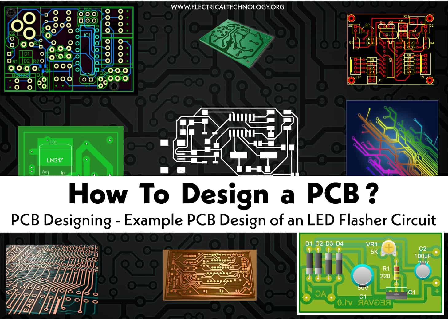
PCB Design Basics: A Comprehensive Introduction
An example Broken Net Marker (top) - a system-generated from-to (connection line) advising how thetwo points should be routed to satisfy topology. DFM is closely related to design for fabrication (DFF) and design for assembly (DFA). Simple, intuitive, well-known user-interface concepts help to get startedwith LibrePCB very quickly. No need to study the documentation for days –just start working with it. Hope this article has given you some good tips and ideas on how to design your next PCB layout!
Fusion 360 is a popular CAD, CAM, CAE, and PCB software from Autodesk. It ships with its own circuit board design software, called Fusion 360 Electronics. But thanks to the buyout of CadSoft, the original developer, Fusion 360 now comes with a standalone PCB design program called Eagle. This list of guidelines is not exhaustive, but they are applicable to traces carrying most of the signals you’ll route throughout your PCB. High speed, low speed, low frequency analog, and RF designs all make use of these PCB routing tips, so get used to implementing these same practices in your PCB layout. As soon as you transfer your schematic data into a new PCB layout, you’ll have to place components around the board.
Connection lines are automatically re-optimized as you move a component. In this manner the connection lines act as a guide to the optimum position and orientation of the component as it is placed. 5) Add connections for the remaining elements of the circuit, as shown in the figure below. When finished placing all connections, right-click or press ESC to exit placement mode. 6) The system remains in component placement mode with the part outline floating on the cursor.
Once everything in the layout is routed and finalized, your job still isn’t finished. As a designer, it’s your job to create manufacturing files from the PCB layout. PCB design software includes tools to create these output files automatically. By default, Altium Designer will maintain thermal connections onto polygons when you create a new project.
Some recommendations state that plane layer placement must be symmetrical, but this is not strictly required for manufacturing. In large boards, this might be needed to reduce the chances of warping, but this is not a concern in smaller boards. Focus on access to power and ground, as well as ensuring all traces have strong return path coupling to the nearest ground plane first, then worry about perfect symmetry in the PCB design stack-up. We are a team of professionals dedicated to providing you with the latest tips, tricks, and techniques for designing and manufacturing printed circuit boards. Gerber files are the standard file format used in the PCB manufacturing process. They contain all the information needed to produce the PCB, including the component placement, trace routing, and copper pouring.
All along, the rules-driven design engine, PCB design tutorial, and online resources will help you stay on track. The first thing you need to check when considering a printed circuit board design software is what operating systems it’s compatible with. For example, if you’re looking for a PCB software for Linux or Mac, you can’t use a program like Altium (which is among the most popular PCB software out there) as it’s only available on Windows. Luckily, programs like Eagle are available on Mac and Linux as well as Windows.
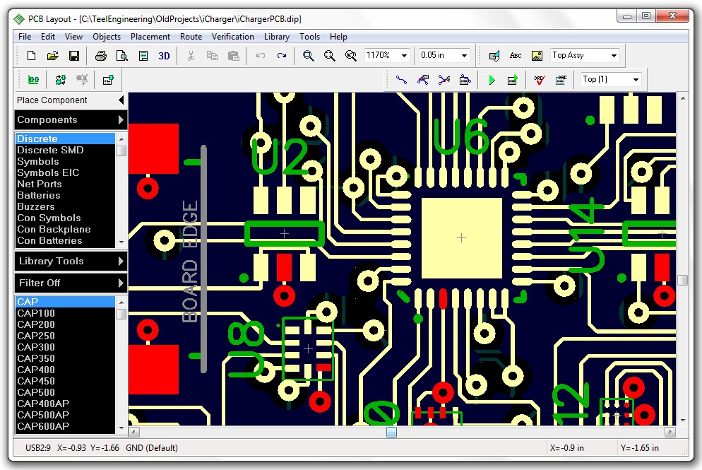
The design files should include all the information and data necessary to build your board; including any notes or special requirements to ensure that your manufacturer is clear on what you require. For most manufacturers, you will be able to use a set of Gerber files as shown below; however, some manufacturers prefer other manufacturing file formats (IPC-2581 or ODB++). It's also important to annotate your schematics, as well as name nets when schematics get large and complex. As higher pin count devices are added to schematics, you can use net name assignments to keep things organized and easily track connectivity between components.


No comments:
Post a Comment